Richard Feynman famously posed the question in 1959: is it possible to see and manipulate individual atoms in materials? For a time his vision seemed more science fiction than science, but starting with groundbreaking experiments in the late 1980s and more recent developments in electron microscopy instrumentation it has become scientific reality. However, damage caused by the electron beam is often an issue in such experiments.
The present study focused on single-layer graphene with silicon atoms embedded into the lattice, previously created and studied by the collaborators from Manchester and Daresbury in the UK. Due to the larger size of silicon compared to carbon, these dopant atoms protrude out from the plane, which makes for interesting dynamics under the electron beam. The detailed simulations performed at the University of Vienna showed that the 60 kiloelectronvolt electrons that the cutting-edge Nion microscopes of both teams use for imaging the structure are not energetic enough to likely cause the outright ejection of atoms, in line with what had been observed.
This is physicist Toma Susi.
(Photo Credit: Peter Rigaud, University of Vienna)
Crucially, however, carbon atoms next to a silicon dopant are slightly less strongly bound, and can receive just enough of a kick to so that they almost escape from the lattice, but are recaptured due to an attractive interaction with the silicon atom. Meanwhile, the silicon relaxes into to the lattice position left empty by the impacted carbon atom, which thus lands back into the lattice on the opposite side from where it started. In effect, the silicon-carbon bond is inverted, which was directly seen by the microscopy teams. Analysing the experimental data of nearly 40 such jumps gave a probability that could be directly compared to the simulations, with remarkable agreement.
Besides being beautiful physics, the findings open promising possibilities for atomic-scale engineering: "What makes our results truly intriguing is that the bond flip is directional – the silicon moves to take the place of the carbon atom that was hit by a probe electron", explains lead author Toma Susi, physicist and FWF Lise Meitner Fellow at the University of Vienna. "This means that it should be possible to control the movement of one or more silicon atoms in the lattice with atomic precision. So perhaps we'll see a new kind of quantum corral or an university logo made of silicon atoms in graphene in the near future", he concludes.
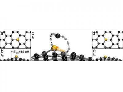
Due to its larger size, a silicon dopant sticks out of the graphene plane.
(Photo Credit: Toma Susi, University of Vienna)
Source: University of Vienna