Lyding and graduate student Scott Schmucker purchased an inexpensive ion gun and tested Lyding's idea. It worked beautifully. STM tips with a starting radius of 100 nanometers were honed to a sharp 1-nanometer point, yielding extremely high resolution. In addition, the sputtering process works with any electrically conductive material.
But once the probes are ultra-sharp, what's to keep them from wearing down just as quickly as other probes? Lyding and Schmucker then teamed with U. of I. chemistry professor Gregory Girolami and materials science and engineering professor John Abelson, whose groups had demonstrated coatings for silicon semiconductors made of a material called hafnium diboride. The coatings are 10 times harder than the metal usually used to make STM tips, but are also metallic – the key property for the ion-sputtering process.
The group applied the hafnium diboride coatings to their probes, sputtered them further, and found that the resulting probes are stable, durable and excel in the types of microscopy and patterning applications for which such tips are used.
"Nobody else makes probes with the combination of sharp, hard and metallic conduction," said Lyding, who is also affiliated with the Beckman Institute for Advanced Science and Technology at the U. of I. "You can find one or the other but not all three. There's a tremendous demand for that."
The researchers now are moving to commercialize their tough, sharp probes. They received a patent and started a company called Tiptek to begin manufacture. They are also expanding their sharpening technique to include AFM probes as well as STM, and are developing batch-processing techniques for higher throughput.
"When people make AFM tips they make them on wafers, hundreds of tips at a time," said Lyding. "The methodology that we're developing lets us process this entire wafer as a unit so all 400 tips would be done at the same time."

Professor Joe Lyding has recently developed a new method for sharpening probes for Scan Probe Microscopes. Using ions to sharpen the tip to an atomic level, the ultrasharp probes allow for an extremely high, atomic resolution in the microscope's images. Hi-res at http://www.youtube.com/watch?v=Wkf2DxbKSFA.
(Photo Credit: Anne Lukeman)
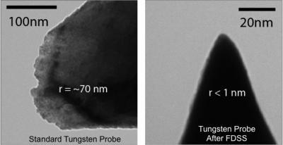
This is a traditionally etched tungsten STM probe (left), sharpened to a 1-nanometer point after bombarding it with ions (right).
(Photo Credit: Joseph Lyding)