Imagine a field of small wires—standing at attention like a tiny field of wheat—gathering the Sun's rays as the first step in solar energy conversion.
Researchers at the University of Illinois at Urbana-Champaign have achieved new levels of performance for seed-free and substrate-free arrays of nanowires from class of materials called III-V (three-five) directly on graphene. These compound semiconductors hold particular promise for applications involving light, such as solar cells or lasers.
"Over the past two decades, research in the field of semiconductor nanowires has helped to reshape our understanding of atomic-scale crystal assembly and uncover novel physical phenomena at the nanometer scale," explained Xiuling Li, a professor of electrical and computer engineering at Illinois. In the March 20th issue of Advanced Materials, the researchers present the first report of a novel solar cell architecture based on dense arrays of coaxial p-n junction InGaAs nanowires on InAs stems grown directly on graphene without any metal catalysts or lithographic patterning.
"In this work, we have overcome the surprising structure (phase segregation) and successfully grown single phase InGaAs and demonstrated very promising solar cell performance," explained postdoctoral researcher Parsian Mohseni, first author of the study.
"Depending on the materials, nanowires can be used for functional electronics and optoelectronics applications," Mohseni added. "The main benefits of this III-V photovoltaic solar cell design are that it is fairly low-cost, substrate-free, and has a built-in back side contact, while being conducive to integration within other flexible device platforms."

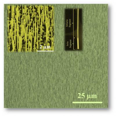
A dense array of nanowires was grown directly on graphene. The insets show a higher magnification SEM view of the array and a STEM image of a single, axially heterostructured InGaAs/InAs nanowires.
(Photo Credit: Parsian Mohseni)
Li's research group uses a method called van der Waals epitaxy to grow nanowires from the bottom up on a two-dimensional sheet, in this case, graphene. Gases containing gallium, indium, and arsenic are pumped into a chamber where the graphene sheet sits, prompting the nanowires self-assemble, growing by themselves into a dense carpet of vertical wires across the graphene's surface.
In their earlier work (Nano Letters 2013) using a graphene sheet, the researchers discovered that InGaAs wires grown on graphene spontaneously segregate into an indium arsenide (InAs) core with an InGaAs shell around the outside of the wire. To improve the materials' efficiencies for solar power conversion, the researchers bypassed the unique van der Waals epitaxy induced spontaneous phase segregation by inserting InAs segments in between. The resulted ternary InGaAs NW arrays are vertical, non-tapered, controllable in size, height, and doping, and broadly tunable in composition thus energy for monolithic heterogeneous integration with 2D van der Waals sheets including graphene.
Under air mass 1.5 global solar illumination, the core-shell In0.25Ga0.75As (Eg ~ 1.1 eV) nanowire arrays on graphene demonstrate a conversion efficiency of 2.51 %, representing a new record for substrate-free, III-V NW-based solar cells.
"Although InGaAs is far from being the optimum bandgap materials for high efficiency solar cells, the direct epitaxy on graphene platform established here has significant implications for a wide variety of III-V compound semiconductor NW based solar cells on graphene, as well as light emitters and multi-junction tandem solar cells, all of which can be released for flexible applications," Li said.

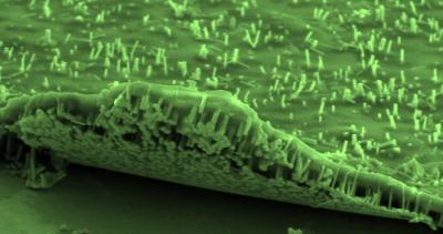
The InGaAs/InAs nanowire array can be lifted from its graphene base and transferred to alternative platforms for bendable device applications.
(Photo Credit: Parsian Mohseni)