Like snowflakes or fingerprints, no two quantum dots are identical. But a new etching method for shaping and positioning these semiconductor nanocrystals might change that. What's more, tests at the National Institute of Standards and Technology (NIST) confirm that etched quantum dots emit single particles of light (photons), boosting prospects for powering new types of devices for quantum communications.
The conventional way to build quantum dots—at NIST and elsewhere—is to grow them like crystals in a solution, but this somewhat haphazard process results in irregular shapes. The new, more precise process was developed by NIST postdoctoral researcher Varun Verma when he was a student at the University of Illinois. Verma uses electron beam lithography and etching to carve quantum dots inside a semiconductor sandwich (called a quantum well) that confines particles in two dimensions. Lithography controls the dot's size and position, while sandwich thickness and composition—as well as dot size—can be used to tune the color of the dot's light emissions.
Some quantum dots are capable of emitting individual, isolated photons on demand, a crucial trait for quantum information systems that encode information by manipulating single photons. In new work reported in Optics Express,* NIST tests demonstrated that the lithographed and etched quantum dots do indeed work as sources of single photons. The tests were performed on dots made of indium gallium arsenide. Dots of various diameters were patterned in specific positions in square arrays. Using a laser to excite individual dots and a photon detector to analyze emissions, NIST researchers found that dots 35 nanometers (nm) wide, for instance, emitted nearly all light at a wavelength of 888.6 nm. The timing pattern indicated that the light was emitted as a train of single photons.
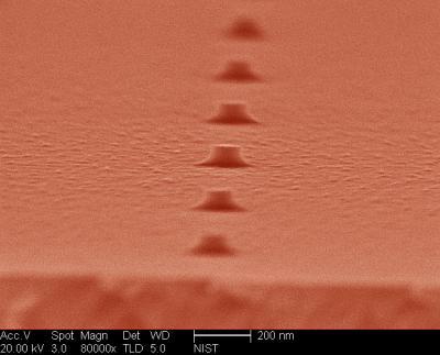
Colorized micrograph of quantum dots made using electron beam lithography and etching. This type of quantum dot can be shaped and positioned more reliably than dots made with conventional crystal growth methods.
(Photo Credit: Verma/NIST)
NIST researchers now plan to construct reflective cavities around individual etched dots to guide their light emissions. If each dot can emit most photons perpendicular to the chip surface, more light can be collected to make a more efficient single photon source. Vertical emission has been demonstrated with crystal-grown quantum dots, but these dots can't be positioned or distributed reliably in cavities. Etched dots offer not only precise positioning but also the possibility of making identical dots, which could be used to generate special states of light such as two or more photons that are entangled, a quantum phenomenon that links their properties even at a distance.
The quantum dots tested in the experiments were made at NIST. A final step was carried out at the University of Illinois, where a crystal layer was grown over the dots to form clean interfaces.
Source: National Institute of Standards and Technology (NIST)