Organic semiconductors allow for flexible displays (OLEDs), solar cells (OPVCs), and other interesting applications. One common problem in these devices, however, is the interface between the metallic contacts and the organic semiconductor material, where undesirable losses occur. Now Dr. Martin Oehzelt has shown what these losses between the metal and the organic semiconductors depend upon and how to minimize them. In particular, his model also explains why a thin, electrically insulating layer between the two materials can even facilitate the transition of charge carriers. His results have recently been published in Nature Communications.
Currently, there are many different approaches describing the interface between organic semiconductor materials and metallic contacts. These somewhat contradictory theories, none of which is universally valid for all cases, have now been unified by Oehzelt and developed into a single coherent model based on the electrostatic potential caused by the charge carriers in the metal and the organic semiconductor. "I calculated the impact of the charge carrier distribution on the electronic states at the interface and how these changes feed back onto the charge carrier distribution", he explains. Oehzelt is presently conducting research with Dr. Georg Heimel as a postdoc for Prof. Norbert Koch, who works at the Humboldt-Universität zu Berlin and the Helmholtz-Zentrum Berlin.
Such calculations have never been so comprehensively carried out before. Performing them, Oehzelt states: "it was surprising to me that the quantum physical level was not that important. The electrostatic effects predominated! The agreement between our model and the experimental data were astonishing." On the example of pentacene, a common organic semiconductor, Oehzelt has quantitatively checked the model's predictions for interface losses.
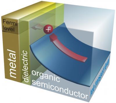
The energy distribution of the electronic states in organic semiconductors determines the minimum energy barrier the charge carriers have to overcome in transitioning from or into the metal. The calculation demonstrates that the shape of this energy barrier can vary, from a step-function to slow, continuously rising curves that lead to considerably lower losses. The latter can be achieved by introducing an extremely thin insulating layer between the organic semiconductor and the metal. Contrary to the general expectation, the introduction of an insulator thus improves the electrical contact.

An ultra-thin dielectric layer can facilitate the extraction of charge carriers (shown here for "holes" in red) from organic semiconductors into metal contacts. It establishes a continuous connection between the energy levels in the organic material (blue) and the metal (black, the Fermi level). This improves electrical contact.
(Photo Credit: M. Oehzelt/HZB)
The results of this work could notably simplify optimization of interfaces and contacts and, thereby, the development of more efficient organic electronic devices.
Source: Helmholtz-Zentrum Berlin für Materialien und Energie