"All we need is these self-propelled nanorobots and UV light," said Jinxing Li, a doctoral student at the Jacobs School of Engineering and first author. "They work together like minions, moving and writing and are easily controlled by a simple magnet."
State-of-art lithography methods such as electron beam writing are used to define extremely precise surface patterns on substrates used in the manufacture of microelectronics and medical devices. These patterns form the functioning sensors and electronic components such as transistors and switches packed on today's integrated circuits. In the mid-20th century the discovery that electronic circuits could be patterned on a small silicon chip, instead of assembling independent components into a much larger "discrete circuit," revolutionized the electronics industry and set in motion device miniaturization on a scale previously unthinkable.
Today, as scientists invent devices and machines on the nanoscale, there is new interest in developing unconventional nanoscale manufacturing technologies for mass production.
Li was careful to point out that this nanomotor lithography method cannot completely replace the state-of-the-art resolution offered by an e-beam writer, for example. However, the technology provides a framework for autonomous writing of nanopatterns at a fraction of the cost and difficulty of these more complex systems, which is useful for mass production. Wang's team also demonstrated that several nanorobots can work together to create parallel surface patterns, a task that e-beam writers cannot perform.
Nanoengineers at the University of California, San Diego recently invented a new method of lithography in which nanoscale robots swim over the surface of light-sensitive material to create complex surface patterns that form the sensors and electronics components on nanoscale devices. Their research, published recently in the journal Nature Communications, offers a simpler and more affordable alternative to the high cost and complexity of current state-of-the-art nanofabrication methods such as electron beam writing.
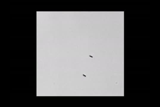
(Photo Credit: Laboratory for Nanobioelectronics, UC San Diego Jacobs School of Engineering)
The team developed two types of nanorobots: a spherical nanorobot made of silica that focuses the light like a near-field lens, and a rod-shape nanorobot made of metal that blocks the light. Each is self-propelled by the catalytic decomposition of hydrogen peroxide fuel solution. Two types of features are generated: trenches and ridges. When the photoresist surface is exposed to UV light, the spherical nanorobot harnesses and magnifies the light, moving along to create a trench pattern, while the rod-shape nanorobot blocks the light to build a ridge pattern.
"Like microorganisms, our nanorobots can precisely control their speed and spatial motion, and self-organize to achieve collective goals," said professor Joe Wang. His group's nanorobots offer great promise for diverse biomedical, environmental and security applications.
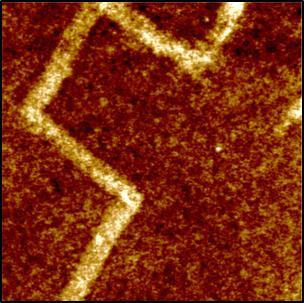
This is an atomic force microscope image of a square-wave pattern written by a rod-shaped nanowire robot for nanoscale device manufacturing.
(Photo Credit: Laboratory for Nanobioelectronics, UC San Diego Jacobs School of Engineering.)
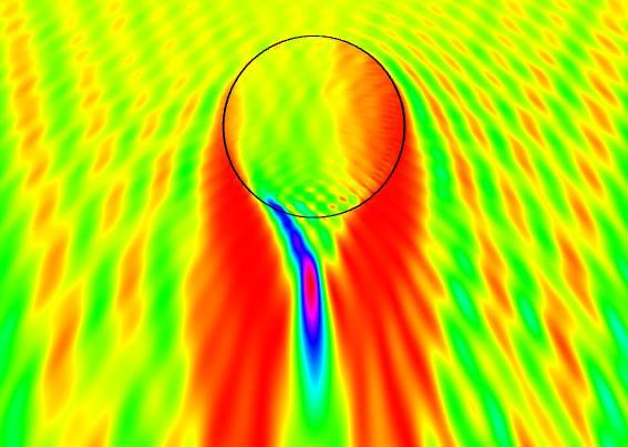
Nanoengineers have invented a spherical nanorobot made of silica that focuses light like a near-field lens to write surface patterns for nanoscale devices. In this image, the red and purple areas indicate where the light is being magnified to produce a trench pattern on light sensitive material. The researchers published their novel "nanomotor lithography" method recently in the journal Nature Communications.
(Photo Credit: Laboratory for Nanobioelectronics, professor Joseph Wang, UC San Diego Jacobs School of Engineering.)